Engineers at Caltech have developed a system of flat optical lenses that can be easily mass-produced and integrated with image sensors, paving the way for cheaper and lighter cameras in everything from cell phones to medical devices.
The technology relies on stacking two metasurfaces. Metasurfaces are sheets of material whose electromagnetic properties can be altered on demand. In this case, the metasurfaces are dotted with silicon cylinders smaller than a micron across that alter the way light passes through them.
"The way we make lenses hasn't changed much since the time of van Leeuwenhoek. Until now," says Caltech's Andrei Faraon (BS '04), referring to Antonie van Leeuwenhoek, a Dutch scientist and lens-maker who created some of the first microscopes.
Faraon, assistant professor of applied physics and materials science in Caltech's Division of Engineering and Applied Science, collaborated with Caltech postdoctoral researcher Amir Arbabi and Seunghoon Han from Samsung Electronics to develop the lens system. Their work was published in Nature Communications on November 28.
A classical lens made of plastic or glass has a curved shape that bends the path of incoming light toward a single focal point. This is because light travels faster through the thinner glass at the edges of the lens than through the thicker glass at the center.
The metasurfaces accomplish the same task using silicon nanoposts, cylinders just 600 nanometers tall and with varying diameters in the hundreds of nanometers. (For scale, a strand of human hair is 100,000 nanometers wide.) Each metasurface is dotted with tens of millions of these posts. Light travels faster through nanoposts with smaller diameters than through nanoposts with larger diameters, so controlling the width of the nanoposts allows the engineers to finely adjust the path of light passing through the metasurface to create flat lenses.
Early experiments with nanopost metasurfaces yielded lenses whose images were blurry around the edges—like a magnifying glass. However, by coupling two metasurfaces together, each nanopost-side-out, the engineers were able to create a lens system that can capture and focus light from a 70-degree angular range, making the technology useful for the first time in microscope and camera imaging applications.
"Metasurfaces like these can be easily mass produced, much the way computer chips are," Arbabi says. "That means this could be a cheap and easily scalable way to create tiny lenses just a few millimeters in diameter."
In addition, the lenses can be seamlessly integrated with CMOS (complementary metal-oxide semiconductor) image sensors because they are made using the same materials and fabrication techniques. CMOS image sensors are the tiny chips that underpin digital photography, and were developed at JPL.
Flat, lightweight, and cheap lenses are in demand for various consumer electronics equipped with cameras, or medical devices such as endoscopes, Faraon says.
Next, the team plans to integrate these lenses into miniaturized cameras and microscopes, and extend their functionality and operation bandwidth.
Their article is titled "Miniature optical planar camera based on a wide-angle metasurface doublet corrected for monochromatic aberrations." Additional coauthors at Caltech are graduate students Ehsan Arbabi, Seyedeh Mahsa Kamali, and Yu Horie. This research was funded by Samsung Electronics, the Defense Advanced Research Projects Agency, the National Science Foundation, and the Department of Energy.
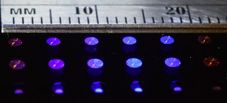
 Flat lenses created by combining two layers of metamaterial studded with silicon nanoposts.
Credit: Caltech
 Two layers of nanoposts yields a wider field of clarity (left), compared to a single layer (right).
Credit: Caltech


