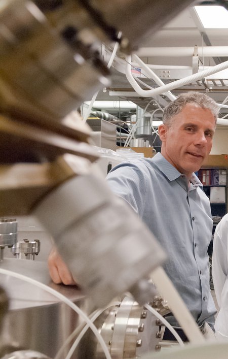
As a high school student during the oil crisis of the 1970s, Harry Atwater recognized firsthand the impact of energy supply issues. Inspired to contribute to renewable energies, his research at Caltech today works to develop better thin-film photovoltaics—cheaper, lighter, more efficient alternatives to the bulky cells now used in solar panels.
In addition to his individual research interests in photovoltaic cell development, Atwater is also part of a collaborative effort to advance solar energy research at the Joint Center for Artificial Photosynthesis (JCAP)—a U.S. Department of Energy (DOE) Energy Innovation Hub. JCAP, which is led by a team of researchers from Caltech and partner Lawrence Berkeley National Laboratory, aims to develop cost-effective fuel production methods that require only sunlight, water, and carbon dioxide.
Atwater, who serves as the project leader for the Membrane and Mesoscale Assembly Project at JCAP, recently chatted with us about his research, his background, and why he came to Caltech.
What originally drew you to Caltech?
It was the opportunity to pursue my area of research. I felt that Caltech was the best research environment I could [be in] for mixing fundamental science and engineering technology. Caltech is very developed in its orientation toward engineering and technology, and its connection to technology in many areas like aerospace, photonics, communications, semiconductors and chemistry. It is a great combination—an institutional focus on fundamentals but also a focus on applying those fundamentals to engineer new technologies.
What are your research interests?
My research is at the intersection of solar energy and nanophotonic materials. Nanophotonic materials are materials and structures in which the characteristic length scale of the material is less than the scale of the wavelength of light—meaning that they're so small that they must be visualized with something that has a wavelength much smaller than that of visual light. Half of my research group is focused on the fundamentals of nanophotonic materials. These materials could form the building blocks of a chip-based optical device technology for improved imaging in computing, communications, and for the detection of chemical and biological molecules.
The other half of my group is focused on improving solar energy. We are investigating several approaches to creating very low-cost and ultrahigh-efficiency thin-film photovoltaics, which are an alternative to, and the future of, today's solar cell panels. In our design, we use thin layers of semiconductors for absorbing sunlight. The Joint Center for Artificial Photosynthesis (JCAP) fundamentally focuses on using semiconductor photonic materials and devices to create fuel from solar energy, so it's a really good match for our work.
How do these semiconductors you're working with make thin-film photovoltaics cheaper, thinner, and more efficient?
Most materials cost nearly the same amount when you just think about them on a price-per-atom basis. What makes materials expensive or cheap is the cost of the synthesis and processing methods used to make them with sufficient purity and perfection to enable high performance. Much of what we do is aimed at either designing new syntheses that can yield high-performance materials in a scalable low-cost fashion or designing new structures and devices whose performance is robust against use of impure or defective materials.
How did you first get interested in your field?
I would say that my interest in solar energy dates back to the first big energy crisis in the 1970s, when I was a high school student. I grew up in Pennsylvania, and I remember my school was shut down for a few weeks in the wintertime because there literally was no oil to heat the burner. I thought then that addressing supplies of energy was an important problem. It made a big impression on me. But at that point, I hadn't really thought about how I could contribute to a solution.
But then in graduate school, I got interested in things at the intersection of physics and electrical engineering, which is really where my work lies. As a graduate student at MIT, I began to focus on developing new technologies for thin-film solar cells. At MIT, I worked in one of the first nanostructure fabrication labs in the country, where it became apparent to me that we could make nanostructures and characterize their properties.
You were among the first scientists to study these nanostructures. What was that like?
Nowadays "nano" is sort of pervasive in the ether—nanomaterials are not unusual. At that time, it was as invisible to the general public as the Internet. It became obvious to me that there was a lot of opportunity to use nanofabrication principles and techniques to make new optical materials. Later, around 2001, we ended up playing a pretty significant role in starting another new field called plasmonics, which studies the behavior of the excitations created by light in metals. This new field led to the first serious and widespread efforts to make these kinds of optical devices and optical materials out of metals.
Do you have any hobbies or interests outside of your research?
I'm an avid soccer player, and I play weekly with the graduate students. Until my kids got to an age when I started embarrassing them, I was coaching them every week. That's what I like to do for fun.
Atwater joined the Caltech faculty as an assistant professor of applied physics in 1988, becoming an associate professor in 1994 and a professor in 1999. Now the Howard Hughes Professor of Applied Physics and Materials Science, Atwater has many roles on campus and beyond. These include serving as the director of the Resnick Sustainability Institute, the director of the Department of Energy's "Light-Material Interactions in Energy Conversion" Energy Frontier Research Center (LMI-EFRC), and most recently as the editor-in-chief of a new research journal, ACS Photonics.
 Harry Atwater, Howard Hughes Professor of Applied Physics and Materials Science
Credit: Lance Hayashida/Caltech Office of Strategic Communications

